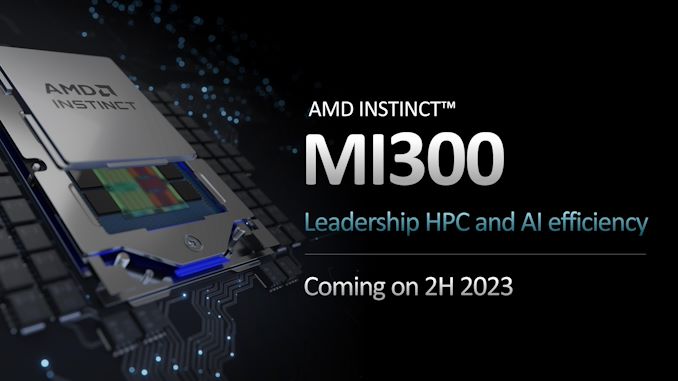
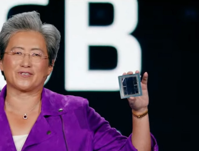
Alongside AMD’s widely expected client product announcements this evening for desktop CPUs, mobile CPUs, and mobile GPUs, AMD’s CEO Dr. Lisa Su also had a surprise up her sleeve for the large crowd gathered for her prime CES keynote: a sneak peak at MI300, AMD’s next-generation data center APU that is currently under development. With silicon literally in hand, the quick teaser laid out the basic specifications of the part, along with reiterating AMD’s intentions of taking leadership in the HPC market.
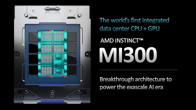
First unveiled by AMD during their 2022 Financial Analyst Day back in June of 2022, MI300 is AMD’s first shot at building a true data center/HPC-class APU, combining the best of AMD’s CPU and GPU technologies. As was laid out at the time, MI300 would be a disaggregated design, using multiple chiplets built on TSMC’s 5nm process, and using 3D die stacking to place them over a base die, all of which in turn will be paired with on-package HBM memory to maximize AMD’s available memory bandwidth.
AMD for its part is no stranger to combining the abilities of its CPUs and GPUs – one only needs to look at their laptop CPUs/APUs – but to date they’ve never done so on a large scale. AMD’s current best-in-class HPC hardware is to combine the discrete AMD Instinct MI250X (a GPU-only product) with AMD’s EPYC CPUs, which is exactly what’s been done for the Frontier supercomputer and other HPC projects. MI300, in turn, is the next step in the process, bringing the two processor types together on to a single package, and not just wiring them up in an MCM fashion, but going the full chiplet route with TSV stacked dies to enable extremely high bandwidth connections between the various parts.
The key point of tonight’s reveal was to show off the MI300 silicon, which has reached initial production and is now in AMD’s labs for bring-up. AMD had previously promised a 2023 launch for the MI300, and having the silicon back from the fabs and assembled is a strong sign that AMD is on track to make that delivery date.
Along with a chance to see the titanic chip in person (or at least, over a video stream), the brief teaser from Dr. Su also offered a few new tantalizing details about the hardware. At 146 billion transistors, MI300 is the biggest and most complex chip AMD has ever built – and easily so. Though we can only compare it to current chip designs, this is significantly more transistors than either Intel’s 100B transistor Xeon Max GPU (Ponte Vecchio), or NVIDIA’s 80B transistor GH100 GPU. Though in fairness to both, AMD is stuffing both a GPU and a CPU into this part.
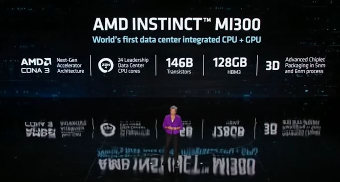
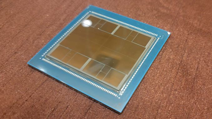
The CPU side of the MI300 has been confirmed to use 24 of AMD’s Zen 4 CPU cores, finally giving us a basic idea of what to expect with regards to CPU throughput. Meanwhile the GPU side is (still) using an undisclosed number of CDNA 3 architecture CUs. All of this, in turn, is paired with 128GB of HBM3 memory.
According to AMD, MI300 is comprised of 9 5nm chiplets, sitting on top of 4 6nm chiplets. The 5nm chiplets are undoubtedly the compute logic chipets – i.e. the CPU and GPU chiplets – though a precise breakdown of what’s what is not available. A reasonable guess at this point would be 3 CPU chiplets (8 Zen 4 cores each) paired with possibly 6 GPU chiplets; though there's still some cache chiplets unaccounted for. Meanwhile, taking AMD’s “on top of” statement literally, the 6nm chiplets would then be the base dies all of this sits on top of. Based on AMD’s renders, it looks like there’s 8 HBM3 memory stacks in play, which implies around 5TB/second of memory bandwidth, if not more.
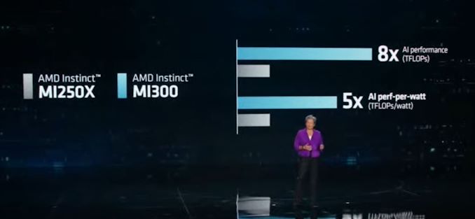
With regards to performance expectations, AMD isn’t saying anything new at this time. Previous claims were for a >5x improvement in AI performance-per-watt versus the MI250X, and an overall >8x improvement in AI training performance, and this is still what AMD is claiming as of CES.
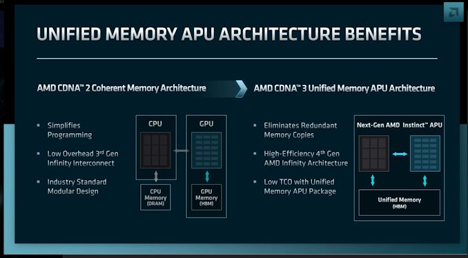
The key advantage of AMD’s design, besides the operational simplicity of putting CPU cores and GPU cores on the same design, is that it will allow both processor types to share a high-speed, low-latency unified memory space. This would make it fast and easy to pass data between the CPU and GPU cores, letting each handle the aspects of computing that they do best. As well, it would significantly simplify HPC programming at a socket level by giving both processor types direct access to the same memory pool – not just a unified virtual memory space with copies to hide the physical differences, but a truly shared and physically unified memory space.
AMD FAD 2022 Slide
When it launches in the later half of 2023, AMD’s MI300 is expected to be going up against a few competing products. The most notable of which is likely NVIDIA’s Grace Hopper superchip, which combines an NVIDIA Armv9 Grace CPU with a Hopper GPU. NVIDIA has not gone for quite the same level of integration as AMD is, which arguably makes MI300 a more ambitious project, though NVIDIA’s decision to maintain a split memory pool is not without merit (e.g. capacity). Meanwhile, AMD’[s schedule would have them coming in well ahead of arch rival Intel’s Falcon Shores XPU, which isn’t due until 2024.
Expect to hear a great deal more from AMD about Instinct MI300 in the coming months, as the company will be eager to show off their most ambitious processor to date.