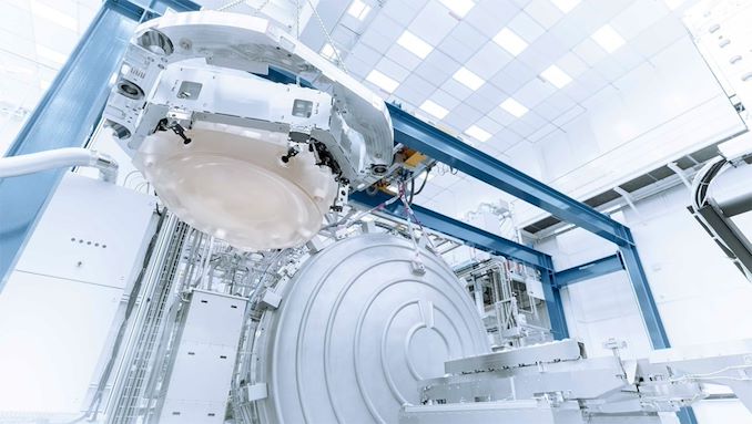
This week ASML is making two very important announcements related to their progress with high numerical aperature extreme ultraviolet lithography (High-NA EUV). First up, the company's High-NA EUV prototype system at its fab in Veldhoven, the Netherlands, has printed the first 10nm patterns, which is a major milestone for ASML and their next-gen tools. Second, the company has also revealed that it's second High-NA EUV system is now out the door as well, and has been shipped to an unnamed customer.
"Our High-NA EUV system in Veldhoven printed the first-ever 10 nanometer dense lines," a statement by ASML reads. "Imaging was done after optics, sensors and stages completed coarse calibration. Next up: bringing the system to full performance. And achieving the same results in the field."
Our High NA EUV system in Veldhoven printed the first-ever 10 nanometer dense lines. ✨ Imaging was done after optics, sensors and stages completed coarse calibration.
Next up: bringing the system to full performance. And achieving the same results in the field. ⚙️ pic.twitter.com/zcA5V0ScUf
— ASML (@ASMLcompany) April 17, 2024
Alongside the system shipped to Intel at the end of 2023, ASML has retained their own Twinscan EXE:5000 scanner at their Veldhoven, Netherlands, facility, which is what the company is using for further research and development into High-NA EUV. Using that machine, the company has been able to print dense lines spaced 10 nanometers apart, which is a major milestone in photolithography development. Previously, only small-scale, experimental lab machines have been able to achieve this kind of a resolution. Eventually, High-NA EUV tools will achieve a resolution of 8 nm, which will be instrumental to build logic chips on technologies beyond 3 nm.
Intel's Twinscan EXE:5000 scanner at its D1X fab near Hillsboro, Oregon is also close behind, and its assembly is said to be nearing completion. That machine will be primarily used for Intel's own High-NA EUV R&D, with Intel slated to use its successor — the commercial-grade Twinscan EXE:5200 — to produce its chips on its Intel 14A (1.4 nm-class) in mass quantities in 2026 – 2027.
But Intel will not be the only chipmaker that gets to experiment with a High-NA EUV scanner for very long. As revealed by ASML, the company recently started shipping another Twinscan EXE:5000 machine to yet another customer. The fab tool maker is not disclosing the client, but previously it has said that all of leading logic and memory producers are in the process of procuring High-NA tools for R&D purposes, so the list of 'suspects' is pretty short.
"Regarding High-NA, or 0.55 NA EUV, we shipped our first system to a customer and this system is currently under installation," said Christophe Fouquet, chief business officer of ASML, at the company's earnings conference call with analysts and investors. "We started to ship the second system this month and its installation is also about to start."
While Intel plans to adopt High-NA EUV tools ahead of the industry, other chipmakers seem to a bit more cautious and plan to rely on risky yet already known Low-NA EUV double patterning method for production a 3 nm and 2 nm. Still, regardless of the exact timing for a transition, all of the major fabs will be relying on High-NA EUV tools in due time. So all parties have an interest in how ASML's R&D turns out.
"The customer interest for our [High-NA] system lab is high as this system will help both our Logic and Memory customers prepare for High-NA insertion into their roadmaps," said Fouquet. "Relative to 0.33 NA, the 0.55 NA system provides finer resolution enabling an almost 3x increase in transistor density, at a similar productivity, in support of sub-2nm Logic and sub-10nm DRAM nodes."
Sources: ASML/X, ASML, Reuters