TSMC has been offering its System-on-Wafer integration technology, InFO-SoW, since 2020. For now, only Cerebras and Tesla have developed wafer scale processor designs using it, as while they have fantastic performance and power efficiency, wafer-scale processors are extremely complex to develop and produce. But TSMC believes that not only will wafer-scale designs ramp up in usage, but that megatrends like AI and HPC will call for even more complex solutions: vertically stacked system-on-wafer designs.

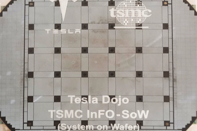
Tesla Dojo's wafer-scale processors — the first solutions based based on TSMC's InFO-SoW technology that are in mass production — have a number of benefits over typical system-in-packages (SiPs), including low-latency high-bandwidth core-to-core communications, very high performance and bandwidth density, relatively low power delivery network impendance, high performance efficiency, and redunancy.
But with InFO-SoW and other wafer scale integration methods, processor designers have to rely solely on on-chip memory. This is perfectly adequate for many applications, but it may not be enough for next-generation AI workloads. Furthermore, with InFO-SoW, the whole wafer has to be processed using one fabrication technology, which may not be optimal, or too expensive for certain designs.

So, with its next-generation system-on-wafer platform, TSMC plans to bring together two of its packaging technologies: InFO-SoW and System on Integrated Chips (SoIC), which will allow it to stack memory or logic on top of a system-on-wafer using its Chip-on-Wafer (CoW) method. The CoW-SoW technology, which the company announced at its North American Technology Symposium, will be ready for mass production in 2027.
For now, TSMC is mostly talking about wedding wafer scale processors with HBM4 memory. And given that HBM4 stacks will feature a 2048-bit interface, its tighter integration with logic is something that the industry is considering.
"So, in the future, using wafer level integrations [will allow] our customers to integrate even more logic and memory together," said Kevin Zhang, Vice President of Business Development at TSMC. "SoW is no longer a fiction, this is something we already work with our customers [on] to produce some of the products already in place. This we think by leveraging our advanced wafer level integration technology, we can provide our customer a very important the path allow them to continue to grow their capability to bring in more computation, more energy efficient computation, to their AI cluster or [supercomputer]."
Related Reading