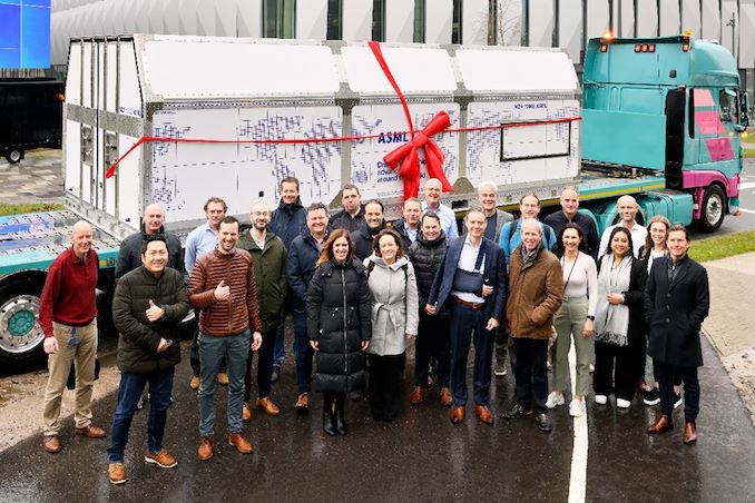
ASML on Thursday said that it had shipped its pilot High-NA EUV scanner to Intel. The Twinscan EXE:5000 extreme ultraviolet (EUV) scanner is AMSL's very first High-NA scanner, and it has eagerly been awaited by Intel, who first placed an order for the machine back in 2018. Intel will be using the new machine to experiment with High-NA EUV before it deploys commercial grade Twinscan EXE:5200 tool for high-volume manufacturing (HVM) sometime in 2025. The announcement represents a major industry milestone that will have an impact not only on Intel, but eventually on the other leading-edge fabs as well.
"We are shipping the first High NA system and announced this in a social media post today," a spokesperson for ASML said. "It goes to Intel as planned and announced earlier."
The ASML Twinscan EXE High-NA scanner is set to make its journey from Veldhoven in the Netherlands all the way to Intel's facility near Hillsboro, Oregon, where the tool, jokingly referred to by Intel CEO Pat Gelsinger as Dr. Ann Kelleher's Christmas present, will be installed in the coming months. It is quite a colossal piece of equipment – so large, in fact, that it requires 13 truck-sized containers and 250 crates just to transport it. And once assembled, the machine is 3 stories tall, which has required Intel to build a new (and taller) fab expansion just to house it. It is estimated that each of these High-NA EUV scanners comes with a hefty price tag, likely in the range between $300 million and $400 million.
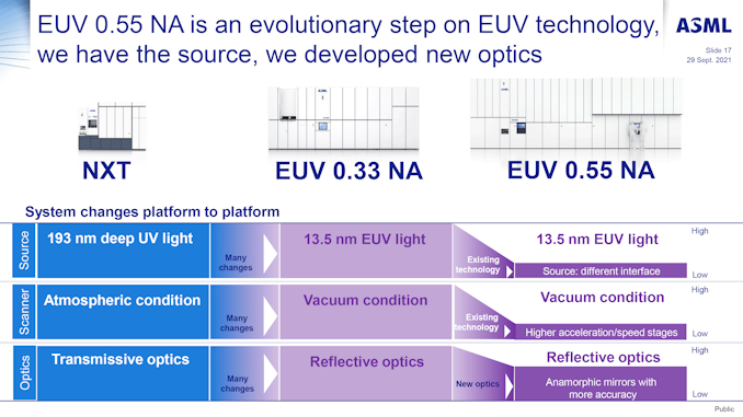
High numerical aperture (High-NA) EUV lithography tools featuring a 0.55 NA lens are capable of an 8nm resolution, which is a significant improvement compared to current EUV tools with a 13nm resolution. These next-generation High-NA EUV scanners are expected to be important for chip production using process technologies beyond 3nm, which the industry is set to adopt in 2025 – 2026, as they will allow fabs to avoid using EUV double patterning, greatly reducing complexity while potentially enhancing yields and lowering costs.

But ASML's Twinscan EXE lithography tools with a 0.55 NA will be significantly different than the company's regular Twinscan NXE litho machines with a 0.33 NA. An avid reader will remember from our previous reports that High-NA scanners are going to be significantly bigger than contemporary EUV scanners, which will require new fab structures. But these is by far not the only difference.
Perhaps the biggest change between the High-NA and regular EUV scanners is the halved reticle size of the High-NA scanners, which will require chipmakers to rethink how they design and produce chips – especially at a time when high-end GPUs and AI accelerators are pushing the limits for reticle sizes. In addition, since High-NA scanners will support a higher resolution and different reticle size, they will require new photoresists, metrology, pellicle materials, masks, and inspection tools, just to name some of the alterations. In short, High-NA tools will require significant investments in infrastructure to go with them.
Although semiconductor production infrastructure is developed by the whole industry, the best way to adopt it for real-world production is to tailor it for actual process technologies and process recipes. Which is why it is so important to start working with pilot scanners early to prepare for HVM using production machines.
Intel was the first company to order ASML's pilot Twinscan EXE:5000 scanner back in 2018. It was also the first to place an order for ASML's commercial grade Twinscan EXE:5200 litho tool in 2022. The company is set to start development work on its 18A node (18 angstroms, 1.8nm) in 2024 and then will employ High-NA tools for a post-18A node, presumably in 2025 – 2026.
By getting High-NA tools earlier than its rivals, Intel not only be able to ensure that its tools produce desired results, but it has a chance to set the standards for the industry when it comes to High-NA manufacturing. For Intel this might mean getting a significant advantage over its rivals, Samsung Foundry and TSMC.
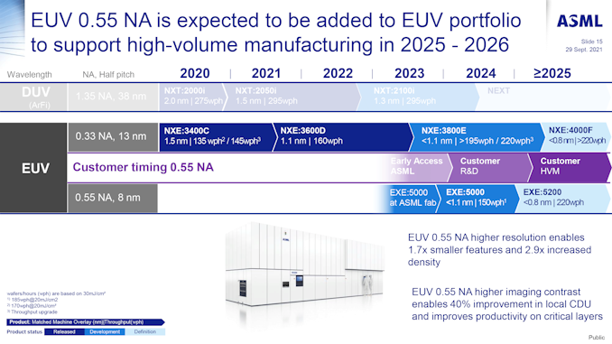
ASML announced in 2022 that it will be able to produce 20 High-NA EUV litho tools per year in 2027 - 2028. Meanwhile, the company disclosed earlier this year is that it had a double-digit number of machines in its High-NA backlog, which signals that its partners are set to adopt these scanners in the coming years. And leading that pack will be Intel.