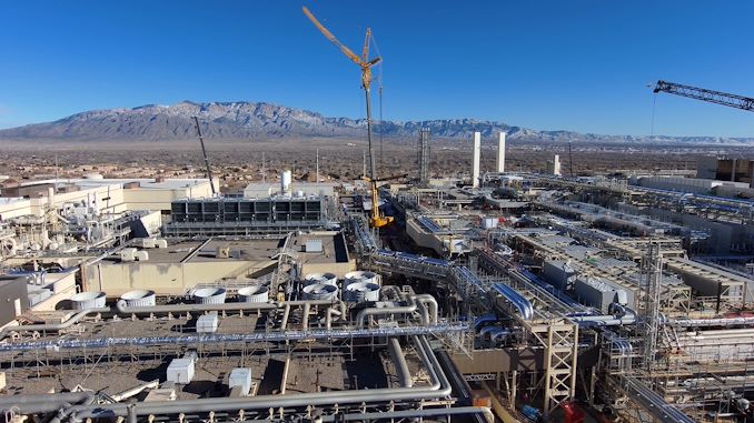
Intel this week has started production at Fab 9, the company's latest and most advanced chip packaging plant. Joining Intel's growing collection of facilities in New Mexico, Fab 9 is tasked with packaging chips using Intel's Foveros technology, which is currently used to build the company's latest client Core Ultra (Meteor Lake) processors and Data Center Max GPU (Ponte Vecchio) for artificial intelligence (AI) and high-performance computing (HPC) applications.
The fab near Rio Rancho, New Mexico, cost Intel $3.5 billion to build and equip. The high price tag of the fab – believed to be the single most expensive advanced packaging facility ever built – underscores just how serious Intel is regarding its advanced packaging technologies and production capacity. Intel's product roadmaps call for making significant use of multi-die/chiplet designs going forward, and coupled with Intel Foundry Services customers' needs, the company is preparing for a significant jump in production volumes for Foveros, EMIB, and other advanced packaging techniques.
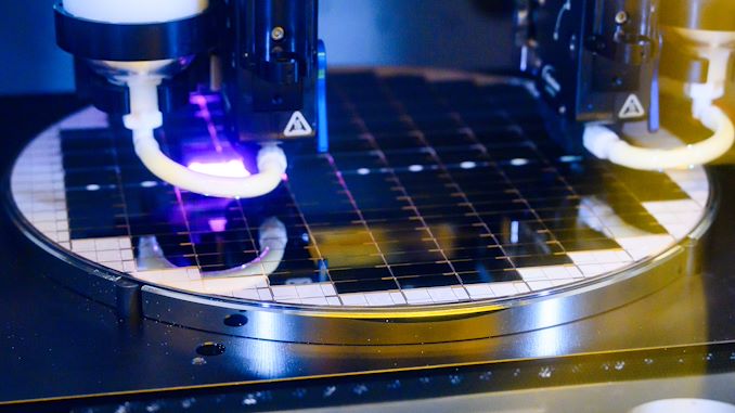
Intel's Foveros is a die-to-die stacking technology that uses a base die produced using the company's low-power 22FFL fabrication process and chiplet dies stacked on top of it. The base die can act like an interconnection between the dies it hosts, or can integrate certain I/O or logic. The current generation Foveros supports bumps that are as small as 36 microns and can enable up to 770 connections per square millimeter, but as the bumps become 25 and 18 microns eventually, the technology will increase connection density and performance (both in terms of bandwidth and in terms of supported power delivery).
A Foveros base die can be as big as 600 mm[SUP]2[/SUP], but for applications that require base dies larger than 600 mm[SUP]2 [/SUP](such as those used for datacenter products), Intel can stitch multiple base dies together using co-EMIB packaging technology.
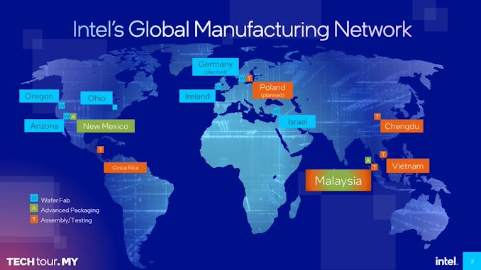
Finally coming into full production, the new Fab 9 (which has inherited its name from what was once a 6-inch wafer lithography fab) is slated to be Intel's crown jewel for Foveros chip packaging for at least the next couple of years. While the company has "advanced packaging" capabilities in Malaysia (PGAT) as well, those facilities are currently only tooled for EMIB production, meaning that all of Intel's Foveros packaging is taking place on its New Mexico campus. As Intel's first high-volume Foveros packaging facility, the additional capacity should greatly expand Intel's total Foveros packaging throughput, though the company isn't providing specific volume figures.
With Intel's Fab 11x directly next door, the pair of facilities are also Intel's first co-located packaging advanced packaging site, allowing Intel to cut down on how many dies they have to import from other Intel fabs. Though as Fab 11x is not an Intel 4 facility, in the case of Meteor Lake it is only suitable for producing the 22FFL base die. Intel is still importing the Intel 4-built CPU die (Oregon & Ireland), as well as the TSMC-manufactured graphics, SoC, and I/O dies (Taiwan).
"Today, we celebrate the opening of Intel's first high-volume semiconductor operations and the only U.S. factory producing the world's most advanced packaging solutions at scale," said Keyvan Esfarjani, Intel executive vice president and chief global operations officer. "This cutting-edge technology sets Intel apart and gives our customers real advantages in performance, form factor and flexibility in design applications, all within a resilient supply chain. Congratulations to the New Mexico team, the entire Intel family, our suppliers, and contractor partners who collaborate and relentlessly push the boundaries of packaging innovation."