
Samsung is set to start making chips using its 2[SUP]nd[/SUP] Generation 3nm-class (SF3) manufacturing technology as well as performance-enhanced version of its 4nm-class (SF4X) fabrication process in the second half of next year, the company told its investors this week. Both production nodes are expected to significantly improve competitive positions of the company as they will enable it to build new types of products.
"We will strengthen our technology competitiveness through the 2H [2023] mass production of the 2nd generation 3nm process as well as the 4[SUP]th[/SUP] generation 4nm process for HPC," a statement by the company reads. "The market is forecast to shift to growth thanks to a rebound in mobile demand and continued growth in HPC demand."
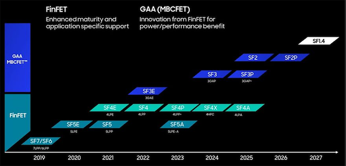
Samsung's forthcoming SF3 process technology is a major upgrade to its existing SF3E production node, which, based on the available knowledge, is only used to make small chips for cryptocurrency mining. Samsung asserts that the SF3 will offer greater design versatility by allowing for different gate-all-around (GAA) transistor's nanosheet channel widths within the same cell type.
Although Samsung does not make direct comparisons between SF3 and SF3E, it says that SF3 offers major improvements over SF4 (4LPP, 4nm-class, low power plus), which includes a 22% increase in performance at equivalent power and complexity, or alternatively, a 34% reduction in power consumption at the same frequency and transistor count, along with a 21% reduction in logic area. In general, it is expected that SF3 will be a better option for complex designs than SF3E, though it will enter high-volume production in the second half of 2024.
In the meantime, Samsung Foundry's 4nm-class generation nodes continue to evolve. The company gearing up to launch its SF4X (4HPC, 4 nm-class high-performance computing) process technology, tailored for high-performance applications such as CPUs and GPUs used in data centers. This one is going to be SF's first process node in recent years that has been specifically designed for high-performance computing (HPC) applications.
Samsung's SF4X process technology promises to deliver a 10% improvement in performance along with a 23% reduction in power consumption. While Samsung has not disclosed the baseline for this comparison, it is likely in reference to their standard SF4 (4LPP) process. This enhancement is achieved through a redesign of the transistor's source and drain regions, following a reassessment of their performance under potentially high-stress conditions, the application of advanced transistor-level design-technology co-optimization (T-DTCO), and the implementation of a new middle-of-line (MOL) architecture.
With refined MOL architecture, SF4X is expected to achieve a silicon-validated minimum operating voltage (Vmin) for CPUs at 60mV, reduce the variability in the off-state current (IDDQ) by 10%, ensure stable high voltage (Vdd) operation above 1V without compromising performance, and enhance process margin for SRAM.