SK hynix this week announced plans to build its advanced memory packaging facility in West Lafayette, Indiana. The move can be considered as a milestone both for the memory maker and the U.S., as this is the first advanced memory packaging facility in the country and the company's first significant manufacturing operation in America. The facility will be used to build next-generation types of high-bandwidth memory (HBM) stacks when it begins operations in 2028. Also, SK hynix agreed to work on R&D projects with Purdue University.
"We are excited to become the first in the industry to build a state-of-the-art advanced packaging facility for AI products in the United States that will help strengthen supply-chain resilience and develop a local semiconductor ecosystem," said SK hynix CEO Kwak Noh-Jung.
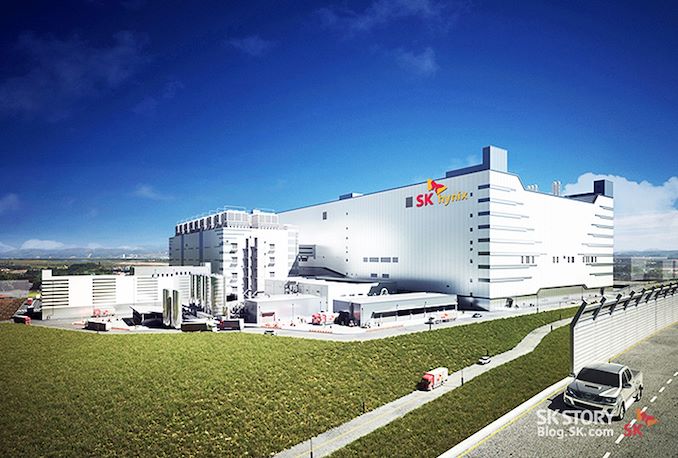
One of The Most Advanced Chip Packaging Facility Ever
The facility will handle assembly of HBM known good stacked dies (KGSDs), which consist of multiple memory devices stacked on a base die. Furthermore, it will be used to develop next-generations of HBM and will therefore house a packaging R&D line. However, the plant will not make DRAM dies themselves, and will likely source them from SK hynix's fabs in South Korea.
The plant will require SK hynix to invest $3.87 billion, which will make it one of the most advanced semiconductor packaging facilities in the world. Meanwhile, SK hynix held the investment agreement ceremony with representatives from Indiana State, Purdue University, and the U.S. government, which indicates parties financially involved in the project, but this week's event did not disclose whether SK hynix will receive any money from the U.S. government under the CHIPS Act or other funding initiatives.
The cost of the facility significantly exceeds that of packaging facilities built by other major players in the industry, such as ASE Group, Intel, and TSMC, which highlights how significant of an investment this is for SK hnix. In fact, $3.87 billion higher than advanced packaging CapEx budgets of Intel, TSMC and Samsung in 2023, based on estimates from Yole Intelligence.
Given that the fab comes online in 2028, based on SK hynix's product roadmap we'd expect that it will be used at least in part to assemble HBM4 and HBM4E stacks. Notably, since HBM4 and HBM4E stacks are set to feature a 2048-bit interface, their packaging process will be considerably more complex than the existing 1024-bit HBM3/HBM3E packaging and will require usage of more advanced tools, which is why it is poised to be more expensive than some existing advanced packaging facilities. Due to the extremely complex 2048-bit interface, many chip designers who are going to use HBM4/HBM4E are expected to integrate it directly onto their processors using hybrid bonding and not use silicon interposers. Unfortunately, it is unclear whether the SK hynix facility will be able to offer such service.
HBM is mainly used for AI and HPC applications, so it is strategically important to have its production in the U.S. Meanwhile, actual memory dies will still need to be made elsewhere, at dedicated DRAM fabs.
Purdue University Collaboration
In addition to support set to be provided by state and local governmens, SK hynix chose to establish its new facility in West Lafayette, Indiana, to collaborate with Purdue University as well as with Purdue's Birck Nanotechnology Center on R&D projects, which includes advanced packaging and heterogeneous integration.
SK hynix intends to work in partnership with Purdue University and Ivy Tech Community College to create training programs and multidisciplinary degree courses aimed at nurturing a skilled workforce and establishing a consistent stream of emerging talent for its advanced memory packaging facility and R&D operations.
"SK hynix is the global pioneer and dominant market leader in memory chips for AI," Purdue University President Mung Chiang said. "This transformational investment reflects our state and university's tremendous strength in semiconductors, hardware AI, and hard tech corridor. It is also a monumental moment for completing the supply chain of digital economy in our country through chips advanced packaging. Located at Purdue Research Park, the largest facility of its kind at a U.S. university will grow and succeed through innovation."