With the arrival of spring comes showers, flowers, and in the technology industry, TSMC's annual technology symposium series. With customers spread all around the world, the Taiwanese pure play foundry has adopted an interesting strategy for updating its customers on its fab plans, holding a series of symposiums from Silicon Valley to Shanghai. Kicking off the series every year – and giving us our first real look at TSMC's updated foundry plans for the coming years – is the Santa Clara stop, where yesterday the company has detailed several new technologies, ranging from more advanced lithography processes to massive, wafer-scale chip packing options.
Today we're publishing several stories based on TSMC's different offerings, starting with TSMC's marquee announcement: their A16 process node. Meanwhile, for the rest of our symposium stories, please be sure to check out the related reading below, and check back for additional stories.
Headlining its Silicon Valley stop, TSMC announced its first 'angstrom-class' process technology: A16. Following a production schedule shift that has seen backside power delivery network technology (BSPDN) removed from TSMC's N2P node, the new 1.6nm-class production node will now be the first process to introduce BSPDN to TSMC's chipmaking repertoire. With the addition of backside power capabilities and other improvements, TSMC expects A16 to offer significantly improved performance and energy efficiency compared to TSMC's N2P fabrication process. It will be available to TSMC's clients starting H2 2026.
TSMC A16: Combining GAAFET With Backside Power Delivery
At a high level, TSMC's A16 process technology will rely on gate-all-around (GAAFET) nanosheet transistors and will feature a backside power rail, which will both improve power delivery and moderately increase transistor density. Compared to TSMC's N2P fabrication process, A16 is expected to offer a performance improvement of 8% to 10% at the same voltage and complexity, or a 15% to 20% reduction in power consumption at the same frequency and transistor count. TSMC is not listing detailed density parameters this far out, but the company says that chip density will increase by 1.07x to 1.10x – keeping in mind that transistor density heavily depends on the type and libraries of transistors used.
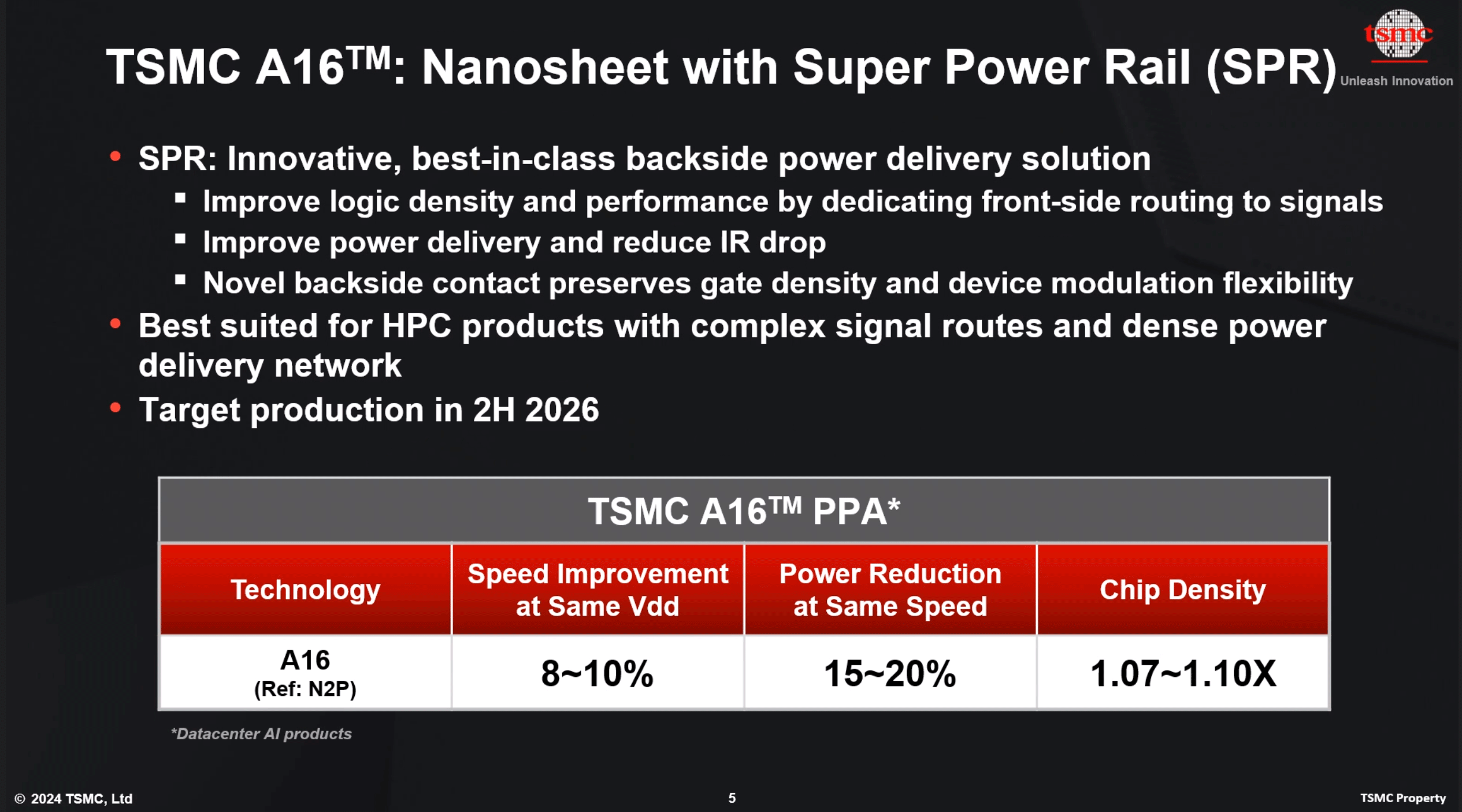
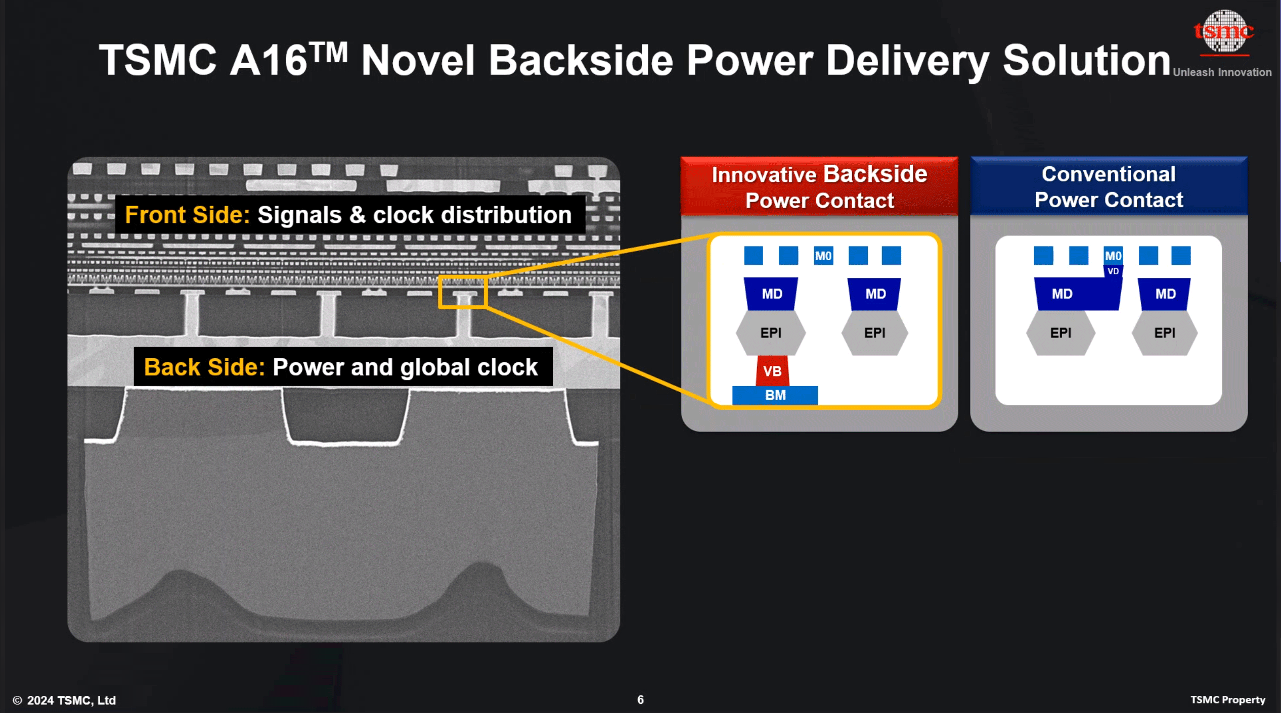
The key innovation of TSMC's A16 node, is its Super Power Rail (SPR) backside power delivery network, a first for TSMC. The contract chipmaker claims that A16's SPR is specifically tailored for high-performance computing products that feature both complex signal routes and dense power circuitry.
As noted earlier, with this week's announcement, A16 has now become the launch vehicle for backside power delivery at TSMC. The company was initially slated to offer BSPDN technology with N2P in 2026, but for reasons that aren't entirely clear, the tech has been punted from N2P and moved to A16. TSMC's official timing for N2P in 2023 was always a bit loose, so it's hard to say if this represents much of a practical delay for BSPDN at TSMC. But at the same time, it's important to underscore that A16 isn't just N2P renamed, but rather it will be a distinct technology from N2P.
TSMC is not the only fab pursuing backside power delivery, and accordingly, we're seeing multiple variations on the technique crop up at different fabs. The overall industry has three approaches for BSPDN: Imec's Buried Power Rail, Intel's PowerVia, and now TSMC's Super Power Rail.
The oldest technique, Imec's Buried Power Rail, essentially places power delivery network on the backside of the wafer and then connects power rail of logic cells to power contact using nano TSVs. This enables some area scaling and does not add too much complexity to production. The second implementation, Intel's PowerVia, connects power to the cell or transistor contact, which provides a better result, but at the cost of complexity.
Finally, we have TSMC's new Super Power Rail BSPDN technology, which connects a backside power network directly to each transistor's source and drain. According to TSMC, this is the most efficient technology in terms of area scaling, but the trade-off is that it's the most complex (and expensive) when it comes to production.
That TSMC has opted to go with the most complex version of BSPDN may be part of the reason that we've seen it removed from N2P, as implementing it will ultimately add to both time and costs. This leaves A16 as TSMC's premiere performance node for the 2026/2027 time-frame, while N2P can be positioned to offer a more balanced combination of performance and cost efficiency.
Angstrom Era Kicks Off In Late 2026 With New Node Naming Convention
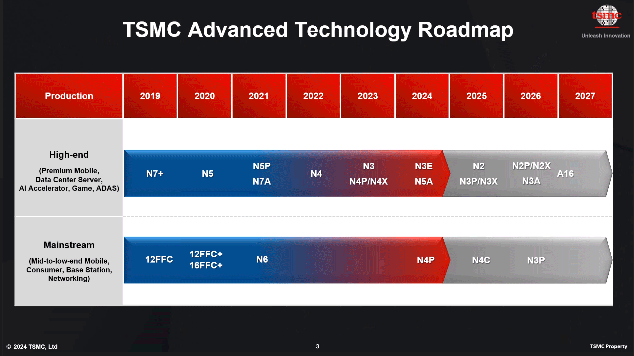
Finally, as with Intel, we're also seeing TSMC adopt a new process node naming convention starting with this generation of technology. The name itself is largely arbitrary – and this has already been the case in the fab industry for several years now – but with current node names already in the single digits (e.g. N2), the industry has needed to re-calibrate node names to something smaller than the nanometer. And thus we've arrived at the 'angstrom era.' But regardless of what exactly it's called or why it's called that, the important point is that A16 will be the next generation node beyond TSMC's 2nm-class products.
TSMC expects to start volume production on A16 in H2 2026, so it is likely that the first products based on this technology will hit the market in 2027. Given the timing, the production node will presumably compete against Intel's 14A; though at 2+ years out and with no one producing BSPDN in volume today, there's still a lot of time for plans and roadmaps to change.
Today we're publishing several stories based on TSMC's different offerings, starting with TSMC's marquee announcement: their A16 process node. Meanwhile, for the rest of our symposium stories, please be sure to check out the related reading below, and check back for additional stories.
Headlining its Silicon Valley stop, TSMC announced its first 'angstrom-class' process technology: A16. Following a production schedule shift that has seen backside power delivery network technology (BSPDN) removed from TSMC's N2P node, the new 1.6nm-class production node will now be the first process to introduce BSPDN to TSMC's chipmaking repertoire. With the addition of backside power capabilities and other improvements, TSMC expects A16 to offer significantly improved performance and energy efficiency compared to TSMC's N2P fabrication process. It will be available to TSMC's clients starting H2 2026.
TSMC A16: Combining GAAFET With Backside Power Delivery
At a high level, TSMC's A16 process technology will rely on gate-all-around (GAAFET) nanosheet transistors and will feature a backside power rail, which will both improve power delivery and moderately increase transistor density. Compared to TSMC's N2P fabrication process, A16 is expected to offer a performance improvement of 8% to 10% at the same voltage and complexity, or a 15% to 20% reduction in power consumption at the same frequency and transistor count. TSMC is not listing detailed density parameters this far out, but the company says that chip density will increase by 1.07x to 1.10x – keeping in mind that transistor density heavily depends on the type and libraries of transistors used.
The key innovation of TSMC's A16 node, is its Super Power Rail (SPR) backside power delivery network, a first for TSMC. The contract chipmaker claims that A16's SPR is specifically tailored for high-performance computing products that feature both complex signal routes and dense power circuitry.
As noted earlier, with this week's announcement, A16 has now become the launch vehicle for backside power delivery at TSMC. The company was initially slated to offer BSPDN technology with N2P in 2026, but for reasons that aren't entirely clear, the tech has been punted from N2P and moved to A16. TSMC's official timing for N2P in 2023 was always a bit loose, so it's hard to say if this represents much of a practical delay for BSPDN at TSMC. But at the same time, it's important to underscore that A16 isn't just N2P renamed, but rather it will be a distinct technology from N2P.
TSMC is not the only fab pursuing backside power delivery, and accordingly, we're seeing multiple variations on the technique crop up at different fabs. The overall industry has three approaches for BSPDN: Imec's Buried Power Rail, Intel's PowerVia, and now TSMC's Super Power Rail.
The oldest technique, Imec's Buried Power Rail, essentially places power delivery network on the backside of the wafer and then connects power rail of logic cells to power contact using nano TSVs. This enables some area scaling and does not add too much complexity to production. The second implementation, Intel's PowerVia, connects power to the cell or transistor contact, which provides a better result, but at the cost of complexity.
Finally, we have TSMC's new Super Power Rail BSPDN technology, which connects a backside power network directly to each transistor's source and drain. According to TSMC, this is the most efficient technology in terms of area scaling, but the trade-off is that it's the most complex (and expensive) when it comes to production.
That TSMC has opted to go with the most complex version of BSPDN may be part of the reason that we've seen it removed from N2P, as implementing it will ultimately add to both time and costs. This leaves A16 as TSMC's premiere performance node for the 2026/2027 time-frame, while N2P can be positioned to offer a more balanced combination of performance and cost efficiency.
Angstrom Era Kicks Off In Late 2026 With New Node Naming Convention
Finally, as with Intel, we're also seeing TSMC adopt a new process node naming convention starting with this generation of technology. The name itself is largely arbitrary – and this has already been the case in the fab industry for several years now – but with current node names already in the single digits (e.g. N2), the industry has needed to re-calibrate node names to something smaller than the nanometer. And thus we've arrived at the 'angstrom era.' But regardless of what exactly it's called or why it's called that, the important point is that A16 will be the next generation node beyond TSMC's 2nm-class products.
TSMC expects to start volume production on A16 in H2 2026, so it is likely that the first products based on this technology will hit the market in 2027. Given the timing, the production node will presumably compete against Intel's 14A; though at 2+ years out and with no one producing BSPDN in volume today, there's still a lot of time for plans and roadmaps to change.